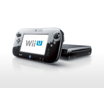
1. Changes in Television
Six years ago, the “Iwata Asks” series began with Iwata Pergunta - Wii1 practically by chance. I never imagined that it would continue this long. Now that we have made a successor console to Wii, I am deeply grateful for this chance to talk again. Today begins a series in which I would like to ask about how the Wii U hardware was made. Thank you for coming today. 1 The first in a series of interviews related to the Wii console that began in late 2006 and led to the continuing “Iwata Asks” series.
Thank you for inviting us.
First, please introduce yourselves. There is no need to introduce Takeda-san again, but he is a person at Nintendo who is responsible for hardware development.
I’m Takeda. Thanks for having me here again.

I’m Shiota from the Product Development Department of the Integrated Research and Development Division. I supervise overall hardware development for such products as the
This time, supervising overall hardware development must have felt like making a home console and a handheld device at the same time! (laughs)
Yes it certainly did! (laughs) I referred to handheld elements while developing the Wii U GamePad, so I feel like I developed two devices, a home console and a handheld at the same time.
I’m Kitano from the Product Development Department of the Integrated Research and Development Division. I was involved in mechanical design for development of the Wii U console. Aside from casing design, I also worked on thermal design and designed elements like the connectors and cables.

I’m Akagi, also from the Product Development Department of the Integrated Research and Development Division. Everyone else worked on the hardware, but I was in charge of software. When I say software, however, I don’t mean software that people play, but rather I was in charge of testing programs necessary in the process of developing the console.
Thank you. When making a new gaming device, what takes the most time is selecting and considering the parts. How did it begin for Wii U?
First of all, for the Japanese TV sets, the transition to digital HD2 terrestrial transmission was completed all over Japan. Much of the world has switched to HD, so you could say that HD has become the new SD3. 2 This term indicates high resolution (high quality images) in televisions and other devices. Conditions for HD include a high number of image pixels, a number of scan lines over 720 pixels, and an aspect ratio of 16:9. Television broadcasting such as ground-wave digital and BS digital that provide high resolution images is called HDTV. 3 This term indicates standard resolution (standard quality images) in televisions and other devices. The number of scan lines is below 720 pixels.
HD has become the standard.
Yes. On the other hand, the Wii console uses SD. The Wii U project kicked off when we thought that we should adjust to the new HD standard for home televisions. Our philosophy is that we want to make something that everyone can enjoy the same way under the same circumstances in many different households.
And the old yellow connector4 for sending video to the television from a video game console changed to HDMI5. In some respects, it was inevitable that if televisions changed, the video game consoles paired with them would also change. 4 One of the RCA connectors (also known as pin jacks) that are generally referred to as a part of a composite cable. It conveys the electrical signals used to connect audio and visual equipment. The connectors are separated by colour, with yellow for composite video signals and red and white for stereo audio signals. 5 This is a standard digital image and sound input/output interface for home appliances and AV equipment. It allows combined sending and receiving of video, audio and control signals with a single cable.
That’s right. And since it’s a device you have in your living room 24 hours a day, we wanted people to be able to enjoy various things aside from games that we couldn’t achieve with Wii. We really had to think a lot to achieve an affordable price while at the same time realising solid performance.
That’s similar to the concept we discussed in the “Wii Hardware” session with regard to low power consumption and high performance6. 6 Takeda-san explained this concept in the “Wii Hardware” session of “Iwata Asks”: “Of course, the issue of performance was not secondary. Anyone can realise low performance with low power. Others tend to aim for high performance with high power. With Wii however, Nintendo alone has pursued high performance with low power consumption.”
Yes. Ever since Nintendo GameCube7, Nintendo has concerned itself with how to improve efficiency by constraining power consumption, and this was in conformity with that idea. 7Nintendo GameCube: A video game console for the home that was first released in Japan in September 2001.
What was the key to achieving low power consumption and high performance this time?
First of all, adoption of a multi-core CPU8 for the first time. By having multiple CPU cores in a single LSI chip, data can be processed between the CPU cores and with the internal high-capacity memory much better, and can now be done very efficiently with low power consumption. 8 A central processing unit (CPU) with multiple processing cores (hardware for running software) for executing commands within a single chip package.
And that we adopted an MCM9. 9 A component with multiple exposed silicon chips called chip pairs on a substrate.
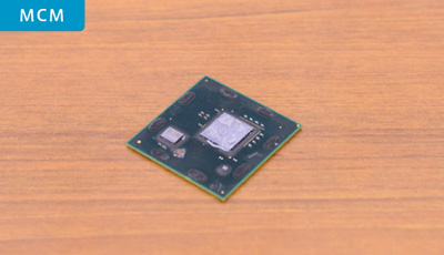
This time we fully embraced the idea of using an MCM for our gaming console. An MCM is where the aforementioned multi-core CPU chip and the GPU chip10 are built into a component. The GPU itself also has quite a lot of memory. Due to this MCM, the cost of the chip package fell and we could speed up data exchange between LSIs while lowering power consumption. And the division of labour made the cost cheaper. 10 Also called a graphics chip or video chip, this is a special chip for rendering computer and game console displays.
A big challenge this time was putting silicon chips made at different semiconductor plants into one package. Shiota-san, as the person who actually had to make that happen, what hurdles did you encounter?
The LSI chips were made at different companies, so when a defect arose, it was difficult to isolate the cause. In defect analysis, it was inside the MCM, so figuring out the problem was incredibly difficult.
When it’s actually running, it’s all inside a single box, so you can’t easily observe what is happening.
Right. We really drew on the wisdom of Renesas11, IBM12 and AMD13, who co-operated with us. To isolate the problem we devised a way to have a minimum amount of signal travel outside of the MCM, so we could verify the signals with the minimum amount of overhead14. 11 A semiconductor manufacturer with its headquarters in Chiyoda Ward, Tokyo. 12 A company providing computer-related services and products. Its headquarters is in New York State. 13 A company that offers development, manufacturing and sales of computer related products. Its headquarters is in the state of California. 14 Excess burden in processing that is ancillary to the original process.
But it must not have been easy to reach that point.
No. We made decisions as we gathered data on our past experiences, but we didn’t notice some things until we actually ran it, so we had to give feedback and repeatedly slog through such areas.
They were different companies, so when it came to defects, it was like, “That isn’t our responsibility.”
Usually when there are defects, you would fix it so it doesn’t happen in the first place. The moment that programmers run a program they have made, they hit the key thinking, “Of course this will run!” And when you tell them it doesn’t run, they think, “It must be a problem somewhere else.” In the same way, when you pack in chips made by different semiconductor manufacturers, it’s only natural for everyone to think, “The problem must be somewhere else.” Shiota-san, how did you handle that?
Simply put, I adopted a policy of “Prove your own innocence.”
Oh, that’s interesting! (laughs)
First, with regard to the LSI chips before inclusion in the package, we tried to establish a way to test without missing anything, and each company devised an extremely robust method. That way they were able to greatly lower the possibility of defects. They were kind enough to provide the all-important information for defect analysis based on the solid data that had built up.
Did that process go smoothly?
It took time to reach that point. At first, there was talk to the effect that if we put in a certain process, we wouldn’t be able to make a lot, or that investment in production facilities would balloon. But if you put your heads together, solutions present themselves, so by fiddling a little with existing test facilities, we found an extremely efficient test pattern and managed to do it.
There still aren’t many instances where all these key components of a system are built into a single chip.
There are a few, but there aren’t many examples of something mass-produced like this with a CPU and GPU of this calibre in one package. This is the MCM substrate.
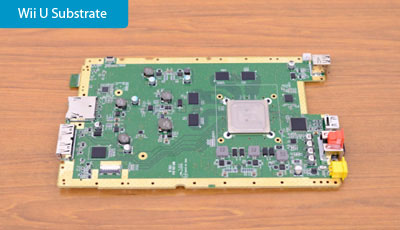
This single chip contains the console’s heart. They were separated into two chips in Nintendo GameCube and Wii. Is the reason you focused on an MCM because you thought the results were worth it?
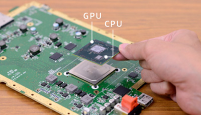
Yes. As Takeda-san said, lowering power consumption has been our position since Nintendo GameCube. By putting LSI chips in this small package, the power necessary for communication between LSI chips drastically fell.
Compared to power flowing between chips in separate physical positions on the board, you can get by with less power inside a small module. The latency is also reduced, and the speed increases.
Yes. And by putting them in a single small package, we can make the footprint on the CPU board smaller. For the contribution it would make to casing miniaturisation too, I wanted to do it no matter what!
